PCB
PCB Board Supply
We do not have any MOQ requirement for PCB products, which helps to save you money and effort. We offer a variety of PCBs and PCB prototypes that are delivered via EMS service, ensuring quick delivery of your PCB product. Thanks to cutting-edge PCB prototyping technology and rich experience, JinHua PCB can be quickly designed and manufactured, with a monthly production capacity of 15,0000 square meters.
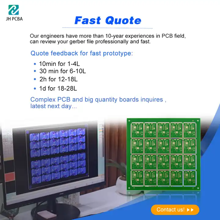
Whether you want to DIY PCB boards, or buy affordable PCBs, quote us, and we will get back to you within 24 hours.
Below you can find a demonstration of our best printed circuit boards.
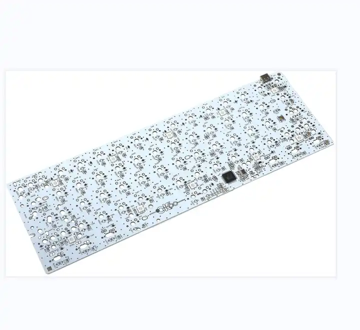
Keyboard PCB
- From $5 for PCB boards
- Lead Time: 1-10 PCS for 3 Days
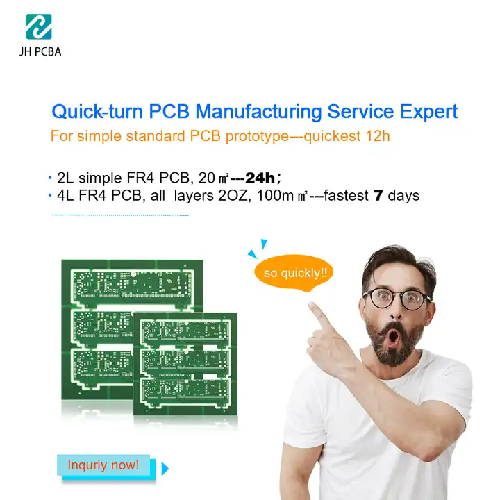
- 24H quickest lead time
- 100% On-time shipping
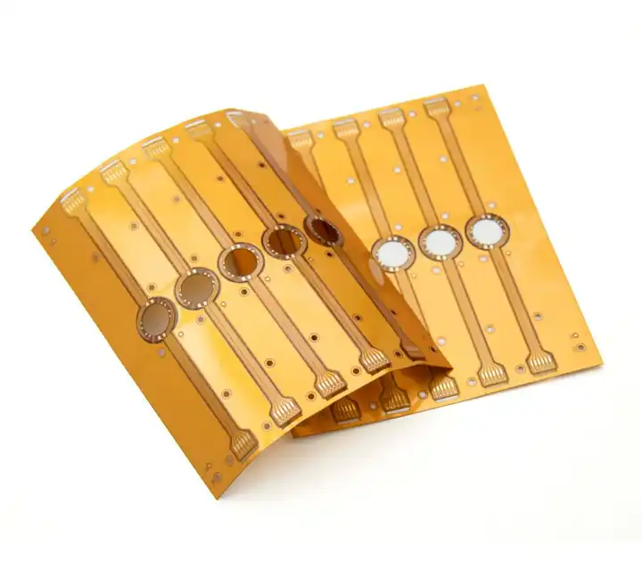
Flex PCB
- From $3.5 for PCB boards
- Lead Time: 1-30 PCB for 5 Days
- Layer: 1-12 Layers
- Board Thickness: Custom
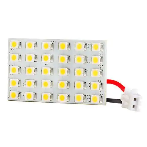
Aluminum PCB
- From $3.5 for PCB boards
- Lead time: 1-100 PCB for 1 Day
- Layer: 1-4 Layers
- Surface Finishing: HAL LF
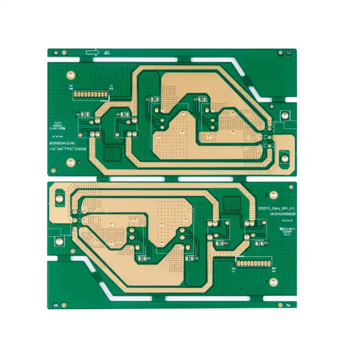
Thick Copper PCB
- From $3.5 for PCB boards
- Lead time: 1-100 PCB for 3 Day
- Layer: 1-20 Layers
- 100% AOI Testing
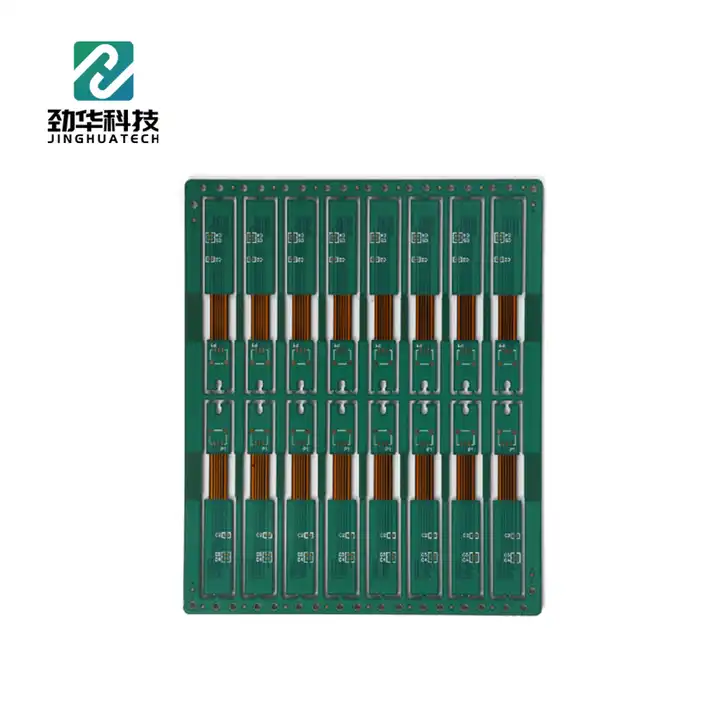
Rigid-flex PCB
- From $3.9 for PCB boards
- Lead time: 1-100 PCB for 3 Day
- Layer: 1-12 Layers
- Base Material: FR4+PI
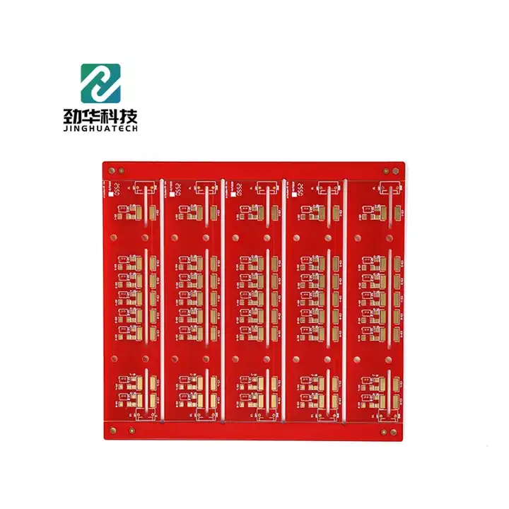
High Frequency PCB
- From $3.9 for PCB boards
- Lead Time: 1-100 PCB for 5 Day
- Layer: 1-20 Layers
- 100% E-Testing
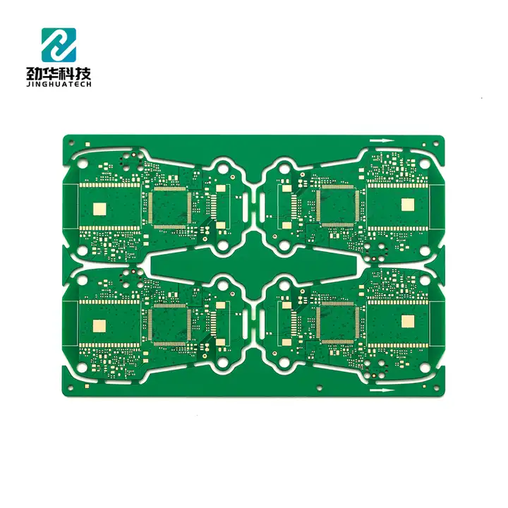
PCB Prototype
- MOQ: 1 Piece
- Lead time: 1-100 PCB for 3 Day
- Layer: 1~32 Layers
- Support Custom Service
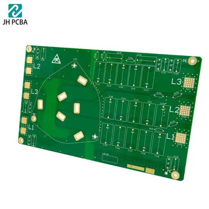
HDI PCB
- From $3.5 for PCB boards
- Lead time: 1-100 PCB for 3 Day
- Layer: 1-20 Layers
- Base Material: FR4
WHY CHOOSE JINHUA
Large PCB Factory
Equipped with advanced production lines and manufacturing equipment, our PCB factory supports different types of PCBs, including rigid PCB, flexible PCB, and rigid-flex circuit boards, which is also extend to various complexities and specifications, such as double-sided PCB, multi-layer PCB, high-frequency PCB, and rapid prototyping of high-tech PCBs. The large PCB factory enables us to handle a wide range of PCB projects, from small-batch orders to large-scale productions.
Advanced PCB Manufacturing Technology
Jinhua boasts cutting-edge PCB technology, such as: HDI(high-density interconnect) technology, which is critical for modern, compact, and high-performance electronic boards; Multiple sequential lamination technology, which is suitable for complex multilayer PCBs.
Excellenct PCB Design
By using advanced PCB layout technology and CAD software, our PCB manufacturing process is efficient and highly precise, allowing to create intricate PCB boards that meet specific requirements, whether for small-scale projects or large, complex systems.
Rapid Prototyping Services
Based on one-stop PCB manufacturing and high-tech equipment, our quick-turn printed circuit boards move swiftly from design to testing, meeting the growing demands of our customers.
Fast Global EMS Delivery
Featuring safe and effencient packaging, EMS delivery enables high-volume PCB products to be delivered in a shorter time, accelerating the shipping of the PCB prototype boards without unnecessary delays.
Custom PCB Service
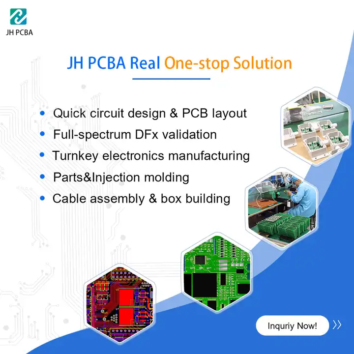
Our PCB design & layout service delivers quick and efficient solutions for your needs.
- Software: Ad, Pro-e, Cam350, Kicad (facilitating the design and simulation of printed circuit board)
- Design Basis: Design instruction, Design rule, customer requirements
- Design Support: PCB design source files, Gerber files, Centroid files, Designator diagrams
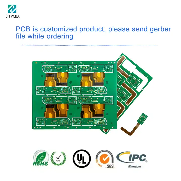
Just send your files of PCB design & layout in the quote.
1.Schematics: DSN and SCH suffixes
2.DXF structure drawing: 2D drawing in AutoCAD format, used to position the device and build board size
3.The component specification: The specification must be with the device size diagram for the establishment and physical one-to-one corresponding package
4.Special requirements
PCB Fabrication
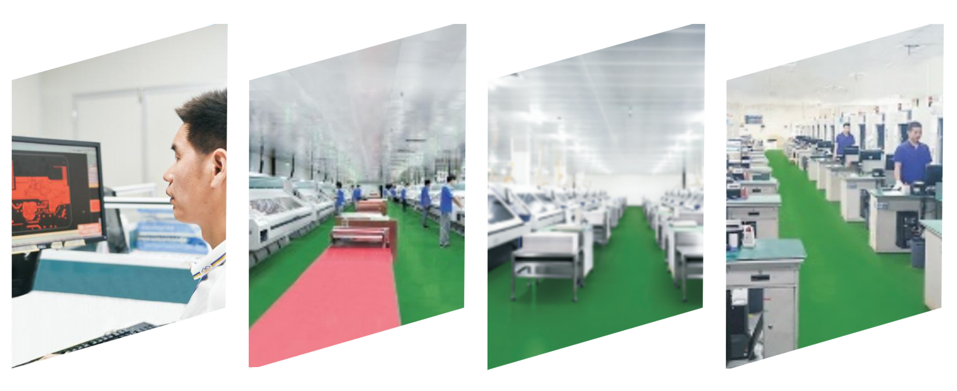
Our high-precision PCB equipment includes: GKG-GSE printing machine, SPI testing equipment, FAI The first tester, Automatic multi-function placement machine, Reflow soldering, AOI equipment and Wave soldering. They enable us to fully optimize the PCB design and meet customer’s unique requirements. Our printed circuit board design services strictly adhere to industry standards for electronics.
PCB Manufacturing Equipment
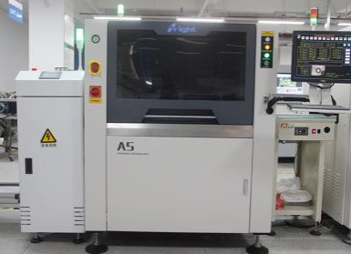
Solder Paste Printer
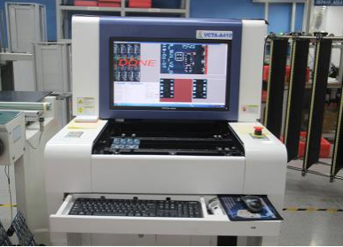
Solder Paste Inspection
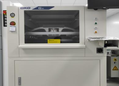
Automatic Solder Paste Printing
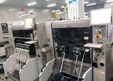
SMT Machine
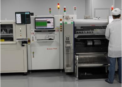
PCB Production Line
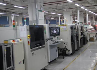
SMT
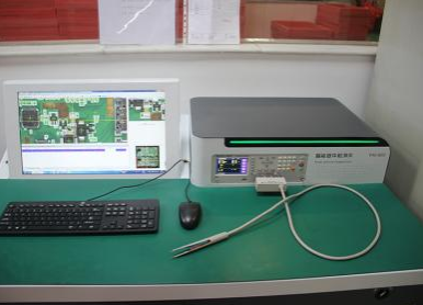
Intelligent Detection Instrument
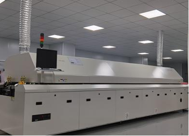
Reflow Soldering

AOI
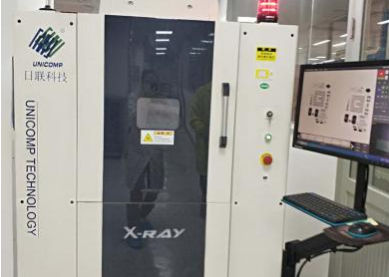
X-Ray
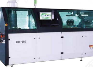
Wave Soldering
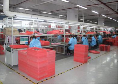
Welding Production Line
PCB Capacity
| PCB Manufaucture | Procedure | |
Solder |
Powder formation | The irregular shape of solder powder will easily clog stencil apertures, which will cause a big slump after printing. It can also cause solder ball and short bridge defects after reflow. A spherical shape is best, especially for fine-pitch QFP printing. |
Particle size | If the particle size is too small, the results will be poor paste adhesion. It will have a high oxygen content and cause a solder ball after reflow. The particle size should be controlled to about 25 ~45 μm in order to meet the requirements for fine-pitch QFP soldering. If the partical size desired is 25 to 30 μm, it should applied with less than 20 μum solder paste for an ultra fine-pitch IC. | |
Particle size | Flux contains a thixotropic agent, which allows the solder paste to have pseudoplastic flow characteristics. Since the viscosity decreases the paste passes through the stencil apertures, the paste can be applied to the PCB pads rapidly. When the external force stops, the viscosity will recover to ensure no deformation occurs. The flux in the solder paste should be controlled to between 8 and 15 percent. A lower flux content will result in excess amount of solder paste applied. Conversely, a high flux content will result in an insufficient amount of solder applied. | |
Stencil |
Thickness | A stencil that is too thick will cause a solder bridge short. A stencil that is too thin will cause an insufficient solder to be applied |
Aperture size | When the stencil aperature size is too big, a solder bridge short can occur. When the stencil aperature size is too small, and insufficient solder paste will be applied. | |
Aperture shape | It is best to use a circular-shaped stencil aperture design. Its size should be slightly smaller than the PCB pad size, preventing a bridging defect during reflow. | |
Printing parameters |
Blade Angle Speed & Pressure | The blade angle affects the vertical force applied on the solder paste. If the angle is too small, the solder paste will not be squeezed into the stencil apertures. The best blade angle should be set around 45 to 60 degrees. A higher the printing speed means that less time will be spent in applying the solder paste through the stencil aperture surface. A higher printing speed will cause insufficient solder to be applied. The speed should be controlled to around 20~40 mm/s.When the blade pressure is too small, it will prevent the solder paste from being cleanly applied to the stencil.When the blade pressure is too high, it will result in more paste leakage. The blade pressure is typically set at about 5N~ 15N / 25mm. |
Printing process control |
PCB moisture | If the PCB moisture is too high, the water under the solder paste will quickly evaporate, causing the solder to splash and creating solder balls.Dry the PCB if it was fabricated over 6 months ago. The recommended drying temperature is 125 degrees for4 hours. |
Paste storage | If the solder paste is applied without a temperature recovery period, the water vapour in the surrounding environment will condense and penetrate the solder paste; this will cause the solder to splash. Solder paste should be stored in a refrigerator at 0 to 5 degrees.Two to fours hours before use, place the paste in a normal temperature environment. | |
PCB Customers
With 14 years of experience, high-precision electronics boards, and quick-turn PCB prototype service, Jinhua is highly recognized by international companies from various industries.
Get A Quote
Wherever you are located in the world – please feel free to ask us anything from a technical question to a quote.

